免费在线3D PCB查看器 — STEP模型逼真渲染
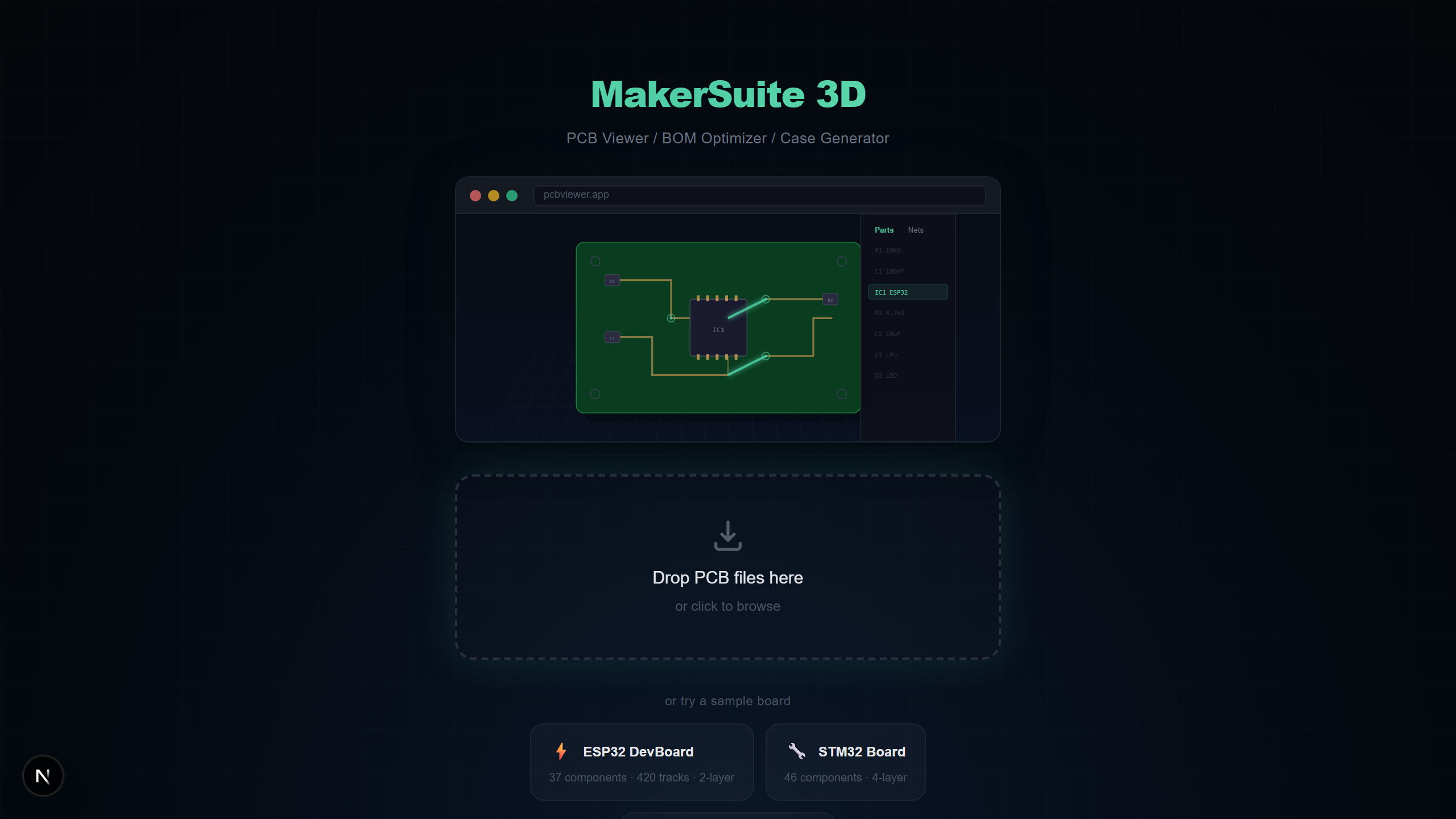
3D PCB查看器有什么不同?
大多数PCB查看器将电路板显示为平面2D图像。3D PCB查看器将这些数据转换为逼真的、可旋转的三维场景,您可以看到元件高度、检查物理间隙,了解组装后电路板的实际外观。MakerSuite 3D使用STEP模型、SSAO和Bloom后处理进一步提升效果——全部在浏览器中运行。
3D可视化对PCB设计的重要性
以3D方式查看PCB不仅仅是为了美观,它解决了2D查看器无法解决的实际工程问题:
- 机械配合验证 — 在订购首个原型前查看高元件是否与外壳壁干涉
- 元件方向检查 — 立即发现旋转的IC或电解电容器极性反转
- 热分析预览 — 识别可能需要散热器间隙或气流空间的元件
- 客户和利益相关者展示 — 向非工程师展示成品电路板的实际外观
- 组装验证 — 将3D渲染与实物电路板进行比较以检查制造错误
如何在线以3D方式查看PCB
使用MakerSuite 3D将PCB转为3D视图只需约5秒:
- 在浏览器中打开pcbviewer.app — 无需安装或注册
- 拖放您的PCB文件(.kicad_pcb、.zip Gerber、.brd、.json或.PcbDoc)
- 查看器在本地解析文件并以3D渲染,包含所有铜层、丝印和元件
- 中键旋转、右键平移、滚轮缩放 — 与Autodesk Inventor相同的控制方式
3D渲染技术
MakerSuite 3D使用React Three Fiber(Three.js)和专业后处理管线提供高质量3D PCB可视化:
- STEP 3D Models — 从Cloudflare R2 CDN加载116+个逼真元件模型,通过IPC-7351封装命名和制造商料号匹配
- SSAO (N8AO) — 屏幕空间环境光遮蔽在元件之间、IC封装下方和电路板边缘添加逼真阴影
- Bloom Glow — 选中的网络以Bloom后处理效果发光,便于在电路板上直观追踪信号路径
- Tone Mapping — ACES电影色调映射确保颜色在不同显示器上看起来自然,不会过度曝光
- 3D Nav Cube — Siemens NX / Autodesk Inventor风格的方向立方体,快速切换相机预设(顶、底、前、后、左、右)
想亲自试试?上传你的 PCB 文件。
免费试用 MakerSuite 3D支持的PCB文件格式
MakerSuite 3D自动检测文件格式并应用正确的解析器。所有解析在浏览器中完成——无需服务器上传:
- KiCad — 包含完整网络数据、多层支持(最多32个铜层)、区域填充和3D模型路径的.kicad_pcb文件
- Gerber — 包含Excellon钻孔的RS-274X Gerber ZIP,自动层检测,可选Pick & Place用于3D元件放置
- Eagle — 包含元件旋转、镜像和丝印文字提取的XML格式.brd文件
- EasyEDA — EasyEDA标准版和LCEDA Pro的JSON格式,自动10mil到mm坐标转换
- Altium — 包含多层支持、盲孔/埋孔和ComponentBodies6流解析的OLE2/CFB二进制.PcbDoc文件
MakerSuite 3D与其他3D PCB查看器对比
以下是MakerSuite 3D与其他提供3D PCB可视化的工具的对比:
- MakerSuite 3D — 免费、浏览器、5种格式、116+ STEP模型、含LCSC/DigiKey/Mouser报价的BOM、Bloom网络高亮、无需注册
- ZofzPCB — 基础使用免费、仅Windows桌面、Gerber输入、3D渲染良好但需安装且无BOM功能
- Altium 365 Viewer — 需Autodesk账户、仅Altium文件、可3D渲染但锁定在Altium生态、无供应商搜索
- KiCad 3D Viewer — 免费、需安装KiCad、仅打开KiCad文件、STEP模型3D出色但无BOM定价集成
- GerbLook — 免费、在线、仅Gerber、仅2D渲染无3D支持、适合快速层检查但功能有限
谁需要3D PCB查看器?
- 无需安装每个工具即可审查使用不同PCB工具的同事设计的硬件工程师
- 通过3D检查元件高度和电路板尺寸来验证外壳配合的机械工程师
- 使用逼真3D可视化探索开源PCB设计的学生和爱好者
- 在3D中查看物理布局的同时检查BOM准确性的采购团队
隐私与安全
MakerSuite 3D使用TypeScript解析器完全在浏览器中处理PCB文件。没有文件数据发送到任何服务器。对于专有设计、NDA保护的项目和数据主权重要的国防电路板都是安全的。
常见问题
What makes a 3D PCB viewer different from a 2D viewer?
A 3D PCB viewer renders your circuit board with realistic depth, component heights, and STEP 3D models. You can rotate the board freely, see how components physically fit together, and inspect clearances that are invisible in flat 2D views. MakerSuite 3D uses Three.js with SSAO and Bloom post-processing for photorealistic rendering.
Can I view Gerber files in 3D?
Yes. MakerSuite 3D parses Gerber RS-274X files with Excellon drill data and reconstructs the board in 3D. If you include a Pick & Place (.pos) file in your ZIP, the viewer also places 3D component models on the board.
How does the 3D model library work?
MakerSuite 3D hosts 116+ STEP 3D models on a Cloudflare R2 CDN. When your PCB is loaded, the viewer matches each component's footprint to the library using IPC-7351 naming (CAPC, RESC, SOP, QFP) and manufacturer part numbers. Components closest to your camera load first.
Is there any file size limit for the 3D viewer?
There is no hard file size limit. Since all parsing happens locally in your browser, performance depends on your device. Boards with 500+ components and 4000+ tracks render smoothly on modern laptops.
How does MakerSuite 3D compare to ZofzPCB and Altium 365 Viewer?
ZofzPCB requires a Windows desktop installation. Altium 365 Viewer requires signup and only opens Altium files. MakerSuite 3D is browser-based, free with no signup, and supports 5 PCB formats (KiCad, Gerber, Eagle, EasyEDA, Altium) with BOM supplier search included.
相关文章
立即以3D方式查看您的PCB
打开 MakerSuite 3D