如何打开Gerber文件 — 完整初学者指南
什么是Gerber文件?
Gerber文件是设计师和制造厂之间传递PCB制造数据的通用标准。在KiCad、Eagle、Altium或任何其他EDA工具中设计PCB后,您会导出Gerber文件发送给制造商。每个Gerber文件描述电路板的一层,钻孔位置存储在配套的Excellon钻孔文件中。这些文件包含工厂制造PCB所需的全部信息。
理解Gerber RS-274X格式
RS-274X扩展Gerber格式由Ucamco维护,自1980年代以来一直是PCB行业标准。以下是关于格式结构需要了解的内容:
- RS-274X — 铜层、阻焊和丝印层的主要格式。使用D代码(D01绘制、D02移动、D03闪烁)和用于走线宽度及焊盘形状的光圈定义。区域(G36/G37)定义铜填充。
- Excellon — 钻孔的单独文件格式。包含工具定义(直径)和每个孔的X/Y坐标。制造商使用它来钻过孔和安装孔。
- 层文件 — 每个PCB层是单独的文件。常见命名:.gtl(顶层铜)、.gbl(底层铜)、.gts(顶层阻焊)、.gbs(底层阻焊)、.gto(顶层丝印)、.gbo(底层丝印)。
- 文件扩展名 — 扩展名因EDA工具而异。KiCad使用.gbr,Eagle使用.cmp/.sol,Altium使用.GTL/.GBL。MakerSuite 3D自动检测所有常见命名模式。
分步:如何在线打开Gerber文件
按照以下步骤在支持3D渲染的免费在线查看器中查看Gerber文件:
- 从PCB设计工具导出Gerber文件(KiCad:文件 > 绘图,Eagle:CAM处理器,Altium:文件 > 制造输出)
- 将所有生成的文件收集到一个ZIP中——包括铜层、阻焊、丝印、轮廓和钻孔(.drl)文件
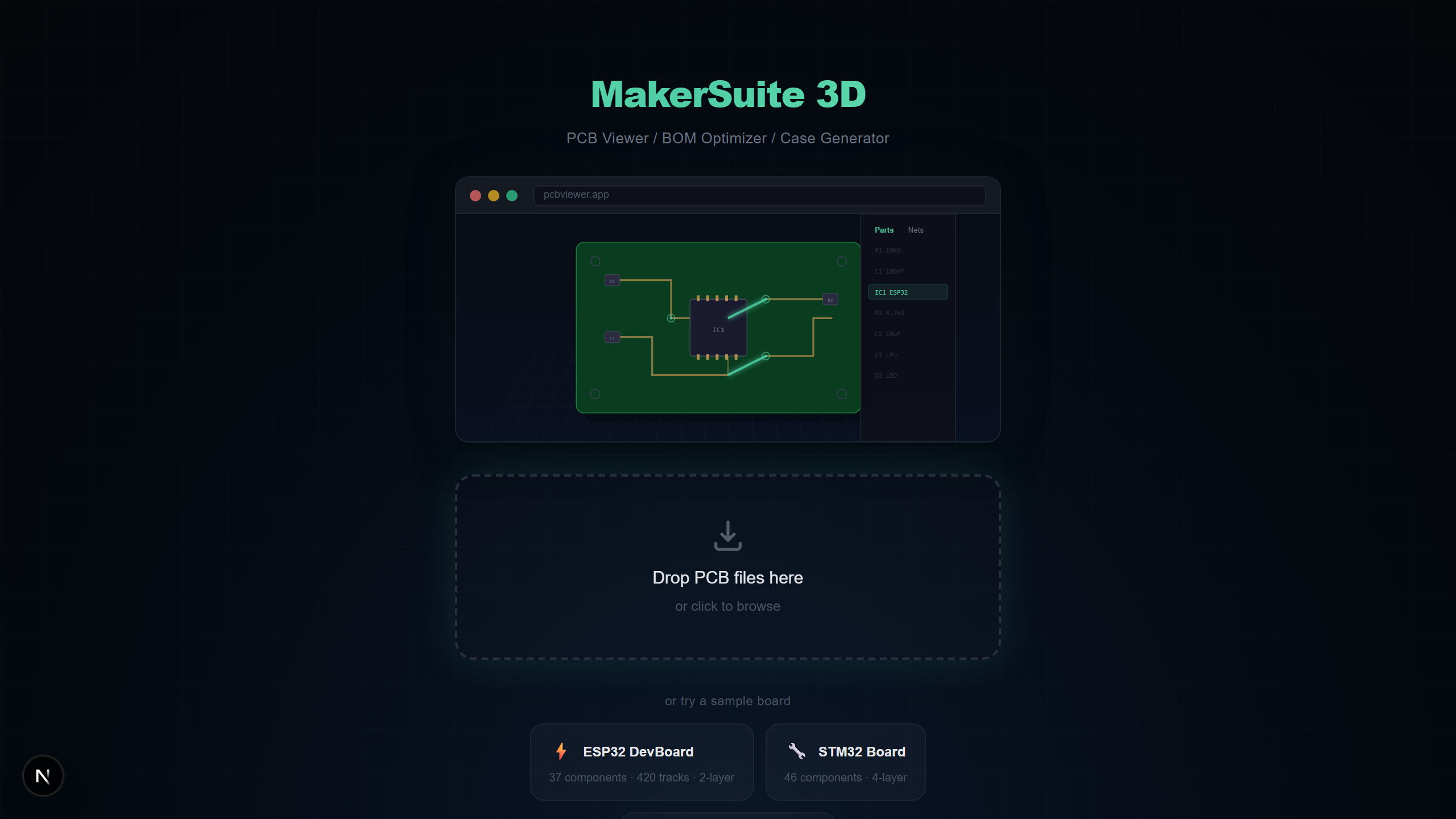
- 打开pcbviewer.app,将ZIP文件拖到放置区
- 层映射对话框出现——MakerSuite 3D自动检测大多数层,您也可以手动重新分配未识别的文件
- 点击应用,您的电路板以铜走线、过孔和板轮廓完整3D渲染
- 可选在ZIP中包含Pick & Place文件(.pos)以在Gerber电路板上看到3D元件模型
Gerber层类型说明
了解每个层文件代表什么有助于在发送制造前验证Gerber输出:
- 铜层 — 定义电气走线、焊盘和铜填充。2层板有顶层(.gtl)和底层(.gbl);4层以上增加内层。
- 阻焊层 — 定义绿色(或其他颜色)保护涂层中焊接开口的位置。顶层阻焊(.gts)和底层阻焊(.gbs)。
- 丝印层 — 包含元件参考标识符(R1、C3、U1)、极性标记和印在电路板表面的组装说明。
- 板轮廓 — 定义PCB的物理形状和尺寸。有时称为Edge.Cuts或机械层。对正确的板形状至关重要。
- 钻孔文件 — Excellon格式,指定过孔、通孔元件和安装孔的孔位置和直径。
想亲自试试?上传你的 PCB 文件。
免费试用 MakerSuite 3D制造前如何检查Gerber文件
向制造商发送不正确的Gerber文件浪费时间和金钱。使用MakerSuite 3D等Gerber查看器在下单前验证这些关键项目:
- 板轮廓与预期尺寸匹配——使用M键测量工具
- 所有铜层都存在且走线正确布线——使用层切换检查每一层
- 钻孔位置正确——在3D视图中检查过孔对齐和安装孔位置
- 阻焊开口露出正确的焊盘——切换阻焊层开/关
- 丝印文字可读且位置正确——验证参考标识符没有与焊盘重叠
Gerber文件查看器选项
多种工具可以打开Gerber文件,各有不同优势:
- MakerSuite 3D — 免费、在线、带自动网络分析的3D渲染、BOM支持、5格式兼容。最适合快速3D检查和BOM核对。
- GerbLook — 免费在线2D Gerber查看器。快速简单但仅限2D和Gerber,无BOM或3D支持。
- ViewMate — Pentalogix的免费Windows桌面应用。2D渲染良好但需安装且仅在Windows上运行。
- KiCad GerbView — KiCad内置的GerbView。需安装KiCad。可靠的2D查看器但Gerber文件无3D渲染。
更好的Gerber文件技巧
- 始终包含Edge.Cuts/板轮廓文件——没有它查看器无法确定板形状
- 将所有文件打包为ZIP一键上传,而不是拖动单个文件
- 如果想在Gerber板上看到3D元件放置,请包含Pick & Place(.pos)文件
- 使用标准扩展名(.gtl、.gbl、.gts、.gbs)命名文件以确保可靠的自动检测
Gerber 导出中会出什么错 — 怎么抓
大多数 Gerber 问题不是格式的错,是导出的错。三个问题占了「我的 fab 订单回来时不对」故事的多数。第一是缺失或命名错误的层 — 每种 EDA 工具对 Gerber 导出包含哪些层有不同的默认值,最常见的缺陷是出货带铜但缺焊膏 mask,或带丝印但缺 paste。第二是 Excellon 钻孔文件中的单位混乱:英寸 vs 毫米、显式小数点 vs 隐式小数点、leading 与 trailing zero suppression。错误组合会产出洞位置大致对但尺寸错的板。第三是完全漏掉板外形(Edge.Cuts)层,让 fab 商从最大的铜多边形猜测您的板形。
MakerSuite 通过渲染 fab 实际会做出什么的 3D 表示来抓住三者。如果顶 mask 层缺失,板子上的每个焊盘都会渲染成被绿色 resist 覆盖 — 视觉上不可能错过的错。如果钻孔单位错了,孔相对于焊盘看起来要么是针眼要么是湖泊,又一次明显。如果板外形缺失,渲染的板形会取最大铜多边形的形状,几乎从不与意图外形匹配。在查看器里抓这些只要 30 秒;板子到货后再抓要重新打样加两周交期。
另一类问题在装配前不可见:与您实际焊接的元件不匹配的焊盘尺寸。查看器不能替代您的 fab 商正经的 DFM 检查,但若包含 Pick & Place 文件,3D 渲染会显示元件落在它们封装上 — 封装错配(0805 焊盘上的 0603 元件,反之亦然)会立刻可见。
拯救板子的下单前清单
在把任何 Gerber 包发给 fab 商之前,在 MakerSuite 里跑这个五点检查。第一,确认板外形。第二,确认层数与意图叠层匹配(4 层板只有 2 个铜 Gerber 表示缺内层)。第三,切换 mask 开关 — mask 开时每个焊盘都应暴露。第四,验证丝印文字可读且不与焊盘重叠。第五,通过寻找落在焊盘外的过孔或与元件引脚不匹配的洞来检查钻孔对齐。
对于发往新 fab 的板子,把同一个 Gerber 包发到第二个查看器(gerblook、KiCad 的 GerbView)做合理性交叉检查。不同查看器暴露不同缺陷 — 在某工具中错命名为铜的层在另一个中可能被标记为 mask,正是您在为 fab 跑付钱前想要的信号。
常见问题
What is a Gerber file?
A Gerber file is the industry-standard format for PCB manufacturing data. It uses RS-274X extended format to describe copper layers, solder mask, silkscreen, and board outlines. Each layer is typically a separate file, and drill data comes in Excellon format.
What programs can open Gerber files?
You can open Gerber files with MakerSuite 3D (free, browser-based, 3D), GerbLook (online, 2D), ViewMate (Windows desktop), KiCad's GerbView, or Altium Designer. MakerSuite 3D is the only free option that renders Gerber files in 3D with automatic net analysis.
Can I view Gerber files without installing software?
Yes. MakerSuite 3D is an online Gerber viewer that runs entirely in your browser. Just ZIP your Gerber files together and drag the ZIP onto pcbviewer.app. No installation, no signup, and your files stay on your device.
How do I check Gerber files before sending them to a manufacturer?
Upload your Gerber ZIP to MakerSuite 3D and verify: (1) all layers are correctly detected, (2) board outline matches your design, (3) drill holes are in the right positions, (4) copper traces look correct in 3D, and (5) silkscreen text is readable. The 3D view makes mechanical fit checks much easier than 2D.
What files should I include in a Gerber ZIP?
Include copper layers (.gtl, .gbl for top/bottom), solder mask (.gts, .gbs), silkscreen (.gto, .gbo), board outline (Edge.Cuts), drill files (.drl), and optionally Pick & Place (.pos) for 3D component placement and a BOM CSV for component values.
相关文章
立即以3D方式打开您的Gerber文件
打开 MakerSuite 3D