下单前如何确认 PCB 可以生产
两天后的那封邮件
失败的过程总是一样:画完板子、跑 DRC、导出 Gerber、上传、付款。两天后工程师发来邮件——第 2 层有最小线宽违规,或者过孔钻径低于我们的下限,或者铜箔离板框太近。于是你要重新改版,交期从头算起。那封邮件里没有任何一条是不可预测的:这些限制全都公布在厂家网站上,也全都能从你已经导出的文件里测出来。
为什么 DRC 通过还不够
DRC 是按项目中配置的设计规则来检查板子的。如果你从默认模板开始,那些规则完全没有包含你最终选定工厂的任何信息。一条 6 mil 的间距规则会永远通过 DRC,无论厂家要求 5 mil 还是 3.5 mil。更麻烦的是,多数新手根本没打开过设计规则对话框,于是 DRC 是在拿软件自带的数字来验证板子。DRC 是必要的——它能抓到任何可制造性检查都不看的短路和未连接网络——但它回答的是关于你意图的问题,而不是关于工厂能力的问题。
真正导致退回的那些数值
实际工作中,少数几项限制几乎占了退回的全部。首先是最小线宽和线距:低于蚀刻极限,走线会变细或短路,再怎么调工艺也救不回来。其次是最小钻孔直径——机械钻孔有下限,低于它就要转向价格档次不同的激光微孔。最容易被忽略的是环宽:钻孔位置有公差,孔周围剩余铜太少时,钻头会从焊盘边缘破出,连接随之失效。再往后是铜箔到板边的距离,因为锣边和 V 割同样有公差,靠近板框的铜箔会被削到或分层。板子尺寸和层数属于代价更低的错误,但同样会挡住订单——叠层由粘合的层对构成,因此奇数层并不存在。
区分外观问题与阻断问题
并非每条警告都该压住订单。丝印问题——比印刷分辨率更细的线条、小到读不清的文字——会让位号变得模糊或消失。这对手工贴装和返修确实不便,但板子照样能做出来、照样能工作。把它们留给下一版处理。铜箔和钻孔违规则不同:那是硬性红线,厂家要么退回文件,要么悄悄替换成你并没有要求的参数。
在浏览器中把你的板子与厂家工艺极限对比——无需上传,无需注册。
免费试用 MakerSuite 3D在浏览器中验证
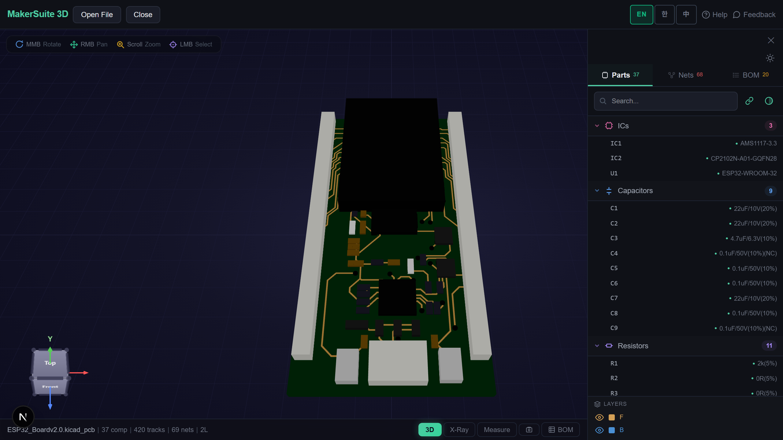
MakerSuite 3D 把整套检查放在客户端运行。把 KiCad、Gerber、Eagle、EasyEDA、Altium、PADS、P-CAD、Protel 99、Allegro 文件拖进查看器,点击工具栏的 DFM,选择厂家。九项检查会依据该厂公布的限制运行,每一项都会给出实测最差值、违规数量和修改方法。点击"在 3D 中显示",所有问题特征都会标注在板子上,回到 EDA 工具时就知道该看哪里。不会上传任何内容——解析和计算都在标签页内完成,设计受保密协议约束时这一点很关键。
仔细读"未评估"
显示为"未评估"的检查项其实在告诉你有用的信息:文件里没有这项数据。导出时没有带 Excellon 钻孔文件的 Gerber 压缩包没有孔可测量,因此无法判断孔径和环宽——把它们报告为通过,比没有结论更糟。缺少板框层时的板边距离也是同理。如果你关心的项目显示"未评估",解决办法是把那一层包含进去重新导出——而这恰恰也是厂家迟早会向你要的。
一分钟的下单前流程
每次下单前:用一个独立于 EDA 工具渲染的查看器打开导出的文件——仅此一步就能发现缺层和板框断裂。按你实际使用的厂家跑 DFM 检查,而不是通用配置。修掉标为失败的项目。记录警告,并有意识地决定现在改还是以后改。然后上传到厂家自己的预览,让他们的内部规则再过一遍。三道关,每道不到一分钟,两天后的那封邮件就不会再来了。
常见问题
Does passing DRC mean my board is manufacturable?
No. DRC compares the board against the design rules configured in your own project, which by default are whatever shipped with the software template. They encode nothing about the factory you eventually chose. A 6 mil clearance rule passes DRC forever, whether the fab needs 5 mil or 3.5 mil on the layer count you ordered. DRC is still necessary because it catches shorts and unconnected nets that no manufacturability check looks at, but it answers a question about your intent rather than the factory's capability.
What are the most common reasons a fab rejects a board?
Trace width and spacing below the etch limit come first — traces neck or short and no process tuning saves them. Then drill diameter under the mechanical floor, which pushes you to laser microvias at a different price tier. Annular ring is the one people forget: drill placement has tolerance, so too little copper around a via means the bit breaks out through the pad edge and the connection dies. After that, copper too close to the board outline, since routing and V-scoring have tolerance too. Board size and layer count are cheaper mistakes but still block an order — odd layer counts do not exist because stackups are built from bonded pairs.
What is a safe minimum annular ring?
0.13 mm is the standard-process floor at both JLCPCB and PCBWay, computed as (pad diameter − drill) / 2. A 0.6 mm pad over a 0.3 mm drill gives 0.15 mm and is comfortably inside spec; a 0.5 mm pad over a 0.3 mm drill gives 0.10 mm and will be flagged. If you are tight on space, enlarging the pad is almost always easier than shrinking the drill, because the drill has its own separate minimum.
Are silkscreen warnings worth fixing before ordering?
Usually not. Lines thinner than the printer resolves and text below roughly 1 mm come out smudged or missing, which makes reference designators useless during hand assembly and rework — but the board is still fabricated and still works electrically. Treat them as a to-do for the next revision. Copper and drill violations are the opposite: hard stops where the fab either rejects the file or silently substitutes a parameter you never asked for.
How do I check a board without installing anything?
Open the board file in MakerSuite 3D's viewer and click DFM in the toolbar, then pick your manufacturer. Nine checks run against that fab's published limits and each reports the worst measured value, the number of violating features, and the fix. "Show in 3D" pins every offending feature onto the board so you know where to look back in your EDA tool. KiCad, Gerber, Eagle, EasyEDA, Altium, PADS, P-CAD and Protel 99 files all work, and nothing is uploaded — parsing and calculation happen in the browser tab.
Why would a check report "not evaluated"?
Because the file does not carry the data for it. A Gerber zip exported without the Excellon drill file has no holes to measure, so hole size and annular ring cannot be judged, and reporting them as passing would be worse than saying nothing. The same applies to edge clearance when the outline layer is missing. If something you care about shows as not evaluated, re-export with that layer included — which is exactly what the fab would have asked you for anyway.
相关文章
别再猜它能不能通过。
运行 DFM 检查