How to View KiCad .kicad_pcb Files in 3D Online

View KiCad PCBs Without Installing KiCad
Need to quickly check a .kicad_pcb file but don't have KiCad installed? MakerSuite 3D lets you view any KiCad PCB file directly in your browser — with full 3D rendering, net highlighting, and component inspection.
Step-by-Step Guide
- Open MakerSuite 3D — Open MakerSuite 3D in your browser
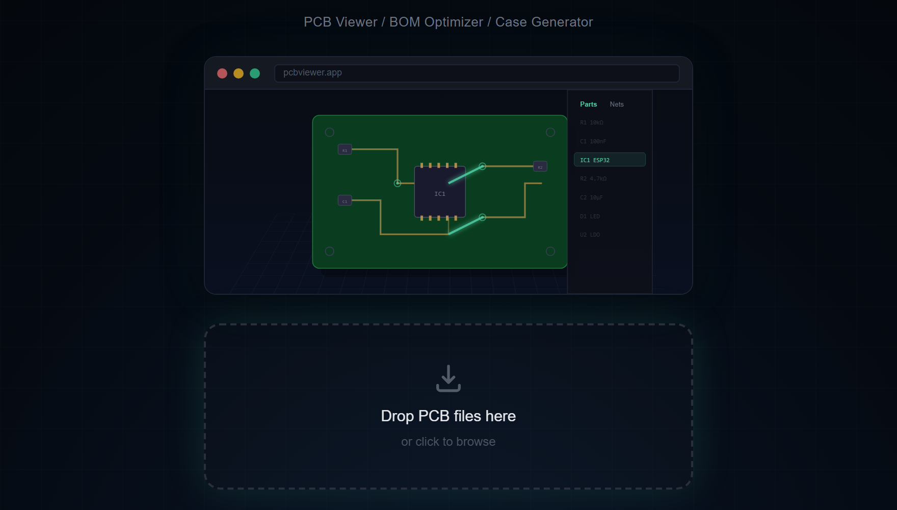
- Drag & drop your .kicad_pcb file onto the viewer
- Explore your PCB in 3D — rotate, pan, zoom
- Click "3D" button to load STEP 3D component models
- Click any net in the sidebar to highlight connected traces
KiCad-Specific Features
- Full net data — All nets from your KiCad design are preserved and clickable
- Multi-layer PCBs — 2, 4, 6, and 8-layer boards with individual layer toggle
- STEP 3D models — 48+ component models (ESP32, SOT-23, SOIC, USB, pin headers, etc.)
- Component sidebar — Browse all components grouped by type (ICs, Capacitors, Resistors...)
- Arc Edge.Cuts — Complex board outlines with arcs, circles, and L-shapes
- Mounting holes — Automatically detected and rendered as board cutouts
Keyboard Shortcuts
- 1-6 — Quick view presets (Top, Bottom, Front, Back, Left, Right)
- X — Toggle X-Ray mode
- M — Measurement tool
- S — Screenshot export
- ESC — Clear selection
See your KiCad board in 3D — no installation required.
Try MakerSuite 3D FreeBOM & Supplier Integration
MakerSuite 3D automatically extracts BOM from your KiCad board. Search LCSC, DigiKey, and Mouser for real-time pricing, compare across suppliers, find alternative parts, and export everything as CSV — directly from the viewer.
New: KiCad Schematic Viewer
MakerSuite 3D now also supports KiCad schematic files (.kicad_sch). View your circuit diagrams alongside your PCB layout — with symbols, wires, power ports, and net labels rendered on a 2D canvas. Features include Parts/Nets sidebar with search, color-coded power ports (VCC in red, GND in blue), PNG export, and keyboard shortcuts. Try it with one of the built-in sample schematics.
Supported KiCad Versions
MakerSuite 3D supports KiCad v4, v5, v6, v7, and v8 .kicad_pcb files. The parser handles both legacy and modern S-expression formats, including v4 center+angle arcs and v6 start+mid+end arcs.
How the .kicad_pcb Format Actually Works
A KiCad PCB file is a single text document written in S-expressions — the parenthesis-heavy syntax inherited from Lisp. Open one in a text editor and you'll see (kicad_pcb (version 20221018) (generator pcbnew) ...) at the top, followed by nested blocks for layers, nets, footprints, segments, vias, and zones. The format is human-readable on purpose: it merges cleanly in git, diffs reasonably in pull requests, and survives forty years from now if every binary tool in your toolchain dies. That's a deliberate design choice, and it's a major reason KiCad has won over teams who care about long-term archival.
MakerSuite parses the entire S-expression tree recursively. The version number at the top (20221018, 20230322, etc.) maps to specific KiCad releases, and the parser branches on a few format quirks: KiCad 4 stored arcs as center-plus-angle while KiCad 6 switched to start-plus-midpoint-plus-end. Both are handled. Layers are identified by their name strings rather than numeric indices, which is how KiCad supports up to 32 copper layers without index collision. Net classes and design rules carry through, so clicking a net in the viewer shows you the same net you'd see in pcbnew.
The 3D model linkage is the part that surprises people. Each footprint in the PCB references a 3D model by file path — typically (model "\${KICAD8_3DMODEL_DIR}/Resistor_SMD.3dshapes/R_0603_1608Metric.step"). Those paths live in the .kicad_pcb file itself, so the viewer can extract them and load the corresponding STEP file from the KiCad CDN automatically. If your design uses a custom 3D library, the path won't resolve and the viewer falls back to a footprint-inferred geometry — which is usually close enough for a layout review.
When Someone Else's KiCad Project Won't Open in pcbnew
If you receive a .kicad_pcb file but pcbnew refuses to open it ("unsupported version" or "file appears corrupt"), the issue is usually a KiCad version mismatch — your pcbnew is older than the file. MakerSuite handles all KiCad versions from 4 through 8, and the parser is forgiving about format quirks that strict pcbnew rejects. Drop the file in the viewer to confirm it's structurally intact before deciding whether to upgrade KiCad or ask for a re-export.
Library-missing warnings are the other common pain. KiCad warns loudly when footprint libraries can't be resolved, even if the layout itself is fine. MakerSuite ignores library resolution and renders directly from the embedded geometry, so you can verify the design looks right even when the libraries are missing — which is the typical state when you receive a project from someone with a different KiCad library setup.
Frequently Asked Questions
Do I need KiCad installed to view .kicad_pcb files?
No. MakerSuite 3D parses KiCad files directly in the browser using a built-in S-expression parser. No software installation needed.
Which KiCad versions are supported?
All versions from KiCad 4 through KiCad 8 are supported, including the latest file format changes and multi-layer boards.
Are 3D STEP models loaded automatically?
Yes. Components are automatically matched to 3D STEP models from a CDN library of 116+ models using IPC-7351 footprint matching and MPN lookup.
Can I view multi-layer PCBs?
Yes. Up to 32 copper layers are supported, including blind and buried vias with proper layer stackup visualization.
Can I view KiCad schematic files too?
Yes. MakerSuite 3D now supports .kicad_sch schematic files with 2D canvas rendering, symbol/wire display, searchable Parts/Nets sidebar, and color-coded power ports.
Related Articles
Try it with your KiCad project
Open MakerSuite 3D