How to Open Gerber Files — Complete Beginner's Guide
What Is a Gerber File?
A Gerber file is the universal standard for communicating PCB manufacturing data between designers and fabrication houses. When you design a PCB in KiCad, Eagle, Altium, or any other EDA tool, you export Gerber files to send to your manufacturer. Each Gerber file describes one layer of your board — the top copper, bottom copper, solder mask, silkscreen, and board outline are all separate files. Drill hole positions are stored in a companion Excellon drill file. Together, these files contain everything a factory needs to fabricate your bare PCB.
Understanding the Gerber RS-274X Format
The RS-274X extended Gerber format is maintained by Ucamco and has been the PCB industry standard since the 1980s. Here is what you need to know about the format structure:
- RS-274X — The main format for copper, mask, and silk layers. Uses D-codes (D01 draw, D02 move, D03 flash) with aperture definitions for trace widths and pad shapes. Regions (G36/G37) define copper fills.
- Excellon — A separate file format for drill holes. Contains tool definitions (diameter) and X/Y coordinates for each hole. Your manufacturer uses this to drill vias and mounting holes.
- Layer files — Each PCB layer is a separate file. Common naming: .gtl (top copper), .gbl (bottom copper), .gts (top mask), .gbs (bottom mask), .gto (top silk), .gbo (bottom silk).
- File extensions — Extensions vary by EDA tool. KiCad uses .gbr, Eagle uses .cmp/.sol, Altium uses .GTL/.GBL. MakerSuite 3D auto-detects all common naming patterns.
Step-by-Step: How to Open Gerber Files Online
Follow these steps to view your Gerber files in a free online viewer with 3D rendering:
- Export Gerber files from your PCB design tool (KiCad: File > Plot, Eagle: CAM Processor, Altium: File > Fabrication Outputs)
- Collect all generated files into a single ZIP — include copper layers, mask, silk, outline, and drill (.drl) files
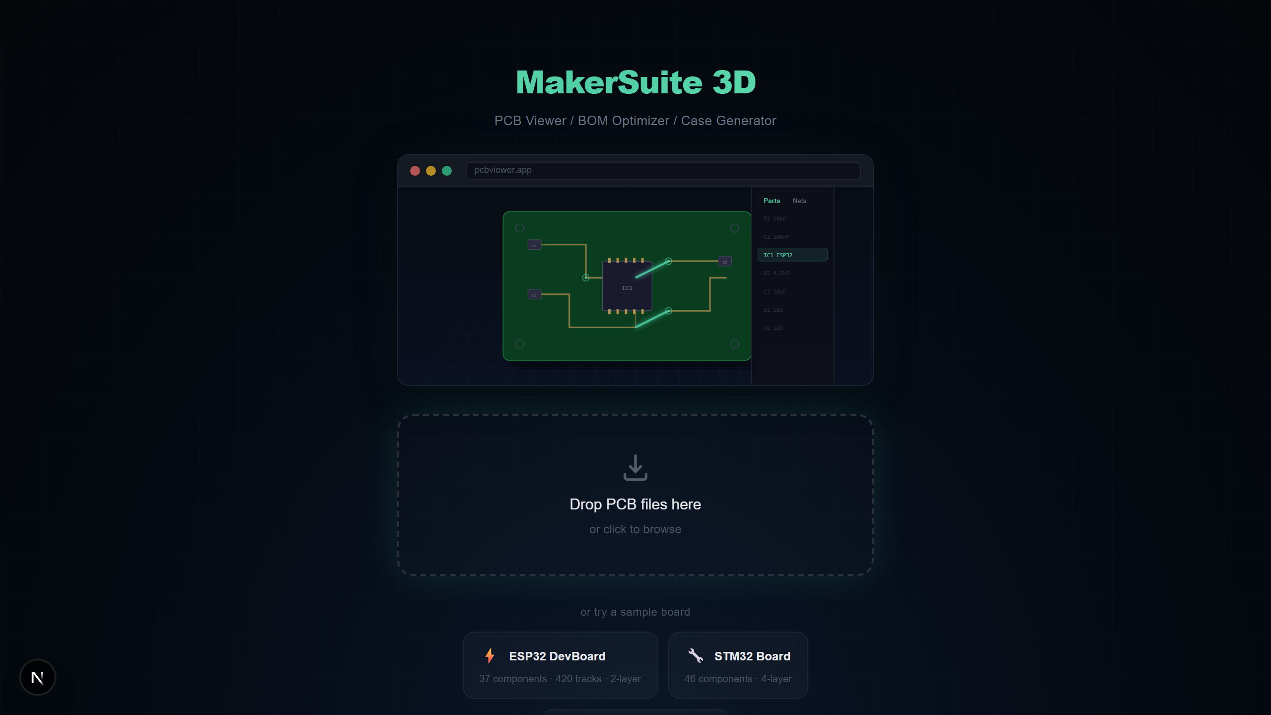
- Open pcbviewer.app and drag your ZIP file onto the drop zone
- The Layer Mapping dialog appears — MakerSuite 3D auto-detects most layers, but you can manually reassign any unrecognized files
- Click Apply and your board renders in full 3D with copper traces, vias, and board outline
- Optionally include a Pick & Place file (.pos) in the ZIP to see 3D component models placed on the board
Gerber Layer Types Explained
Understanding what each layer file represents helps you verify your Gerber output before sending it to manufacturing:
- Copper layers — Define the electrical traces, pads, and copper fills. Top (.gtl) and bottom (.gbl) for 2-layer boards; inner layers for 4+ layer stackups.
- Solder mask — Defines where the green (or other color) protective coating has openings for soldering. Top mask (.gts) and bottom mask (.gbs).
- Silkscreen — Contains component reference designators (R1, C3, U1), polarity marks, and assembly instructions printed on the board surface.
- Board outline — Defines the physical shape and dimensions of the PCB. Sometimes called Edge.Cuts or mechanical layer. Critical for correct board shape.
- Drill files — Excellon format specifying hole positions and diameters for vias, through-hole components, and mounting holes.
Want to try it yourself? Upload your PCB file now.
Try MakerSuite 3D FreeHow to Check Gerber Files Before Manufacturing
Sending incorrect Gerber files to a manufacturer wastes time and money. Use a Gerber viewer like MakerSuite 3D to verify these critical items before placing your order:
- Board outline matches your intended dimensions — measure using the M key tool
- All copper layers are present and traces are correctly routed — use layer toggle to inspect each layer
- Drill holes are positioned correctly — check via alignments and mounting hole locations in 3D view
- Solder mask openings expose the correct pads — toggle the mask layer on/off
- Silkscreen text is readable and correctly positioned — verify reference designators are not overlapping pads
Gerber File Viewer Options
Several tools can open Gerber files, each with different strengths:
- MakerSuite 3D — Free, online, 3D rendering with automatic net analysis, BOM support, and 5-format compatibility. Best for quick 3D inspection and BOM checking.
- GerbLook — Free online 2D Gerber viewer. Fast and simple but limited to 2D and Gerber-only with no BOM or 3D support.
- ViewMate — Free Windows desktop application by Pentalogix. Good 2D rendering but requires installation and only runs on Windows.
- KiCad GerbView — GerbView built into KiCad. Requires KiCad installation. Solid 2D viewer but no 3D rendering for Gerber files.
Tips for Better Gerber Files
- Always include an Edge.Cuts / board outline file — without it, the viewer cannot determine your board shape
- ZIP all files together for one-click upload instead of dragging individual files
- Include a Pick & Place (.pos) file if you want to see 3D component placement on your Gerber board
- Name your files using standard extensions (.gtl, .gbl, .gts, .gbs) for reliable auto-detection
What Goes Wrong With Gerber Exports — and How to Catch It
Most Gerber problems are not the format's fault, they're the export's fault. Three issues account for the majority of "my fab order came back wrong" stories. The first is missing or misnamed layers — every EDA tool has a different default for which layers it includes in a Gerber export, and the most common defect is shipping copper without solder mask, or silk without paste. The second is unit confusion in the Excellon drill file: inch vs millimeter, decimal point vs implicit decimal, leading vs trailing zero suppression. Picking the wrong combination produces a board with holes in approximately the right places but at the wrong sizes. The third is missing the board outline (Edge.Cuts) layer entirely, which leaves the fabricator guessing your board's shape from the largest copper polygon.
MakerSuite catches all three by rendering a 3D representation of what the fabricator will actually build. If your top mask layer is missing, every pad on the board renders as covered with green resist — visually wrong in a way that's impossible to miss. If your drill units are off, the holes appear as either pinpricks or lakes relative to the pads, again obvious. If the board outline is missing, the rendered board takes the shape of the largest copper polygon, which almost never matches your intended outline. Catching these in the viewer takes thirty seconds; catching them after the boards arrive takes a re-spin and another two-week lead time.
The other category of problem is invisible until assembly: pad sizes that don't match the components you'll actually solder on. The viewer doesn't replace a proper DFM check from your fabricator, but with a Pick & Place file included, the 3D render shows components seated on their footprints — and a footprint mismatch (an 0603 component on an 0805 pad, or vice versa) becomes immediately visible.
A Pre-Order Checklist That Saves Boards
Before sending any Gerber package to a fabricator, run this five-point check in MakerSuite. First, confirm the board outline. Second, confirm layer count matches your intended stackup (a 4-layer board with only 2 copper Gerbers is missing inner layers). Third, toggle solder mask on and off — every pad should be exposed when mask is on. Fourth, verify silk text is readable and not overlapping pads. Fifth, check drill alignment by looking for vias that fall outside their pads or holes that don't match component leads.
For boards going to a new fabricator, send the same Gerber package to a second viewer (gerblook, KiCad's GerbView) for a sanity cross-check. Different viewers expose different defects — a layer that misnames as copper in one tool might be flagged as mask in another, which is exactly the signal you want before paying for a fab run.
Frequently Asked Questions
What is a Gerber file?
A Gerber file is the industry-standard format for PCB manufacturing data. It uses RS-274X extended format to describe copper layers, solder mask, silkscreen, and board outlines. Each layer is typically a separate file, and drill data comes in Excellon format.
What programs can open Gerber files?
You can open Gerber files with MakerSuite 3D (free, browser-based, 3D), GerbLook (online, 2D), ViewMate (Windows desktop), KiCad's GerbView, or Altium Designer. MakerSuite 3D is the only free option that renders Gerber files in 3D with automatic net analysis.
Can I view Gerber files without installing software?
Yes. MakerSuite 3D is an online Gerber viewer that runs entirely in your browser. Just ZIP your Gerber files together and drag the ZIP onto pcbviewer.app. No installation, no signup, and your files stay on your device.
How do I check Gerber files before sending them to a manufacturer?
Upload your Gerber ZIP to MakerSuite 3D and verify: (1) all layers are correctly detected, (2) board outline matches your design, (3) drill holes are in the right positions, (4) copper traces look correct in 3D, and (5) silkscreen text is readable. The 3D view makes mechanical fit checks much easier than 2D.
What files should I include in a Gerber ZIP?
Include copper layers (.gtl, .gbl for top/bottom), solder mask (.gts, .gbs), silkscreen (.gto, .gbo), board outline (Edge.Cuts), drill files (.drl), and optionally Pick & Place (.pos) for 3D component placement and a BOM CSV for component values.
Related Articles
Open your Gerber files in 3D right now
Open MakerSuite 3D