How to Check if Your PCB Is Manufacturable Before Ordering
The Two-Day Email
The failure mode is always the same. You finish the board, run DRC, export Gerbers, upload, pay. Two days later an engineer emails you: minimum trace width violation on layer 2, or the drill on your via is under our limit, or copper too close to the board outline. Now you are re-spinning the board and the lead time restarted. None of that email was unpredictable — every one of those limits is published on the fab's website, and every one of them is measurable from the files you already exported.
Why DRC passing is not enough
DRC checks your board against the design rules configured in your project. If you started from a default template, those rules encode nothing about the factory you eventually chose. A 6 mil clearance rule passes DRC forever, whether the fab needs 5 mil or 3.5 mil. Worse, most beginners never open the design rules dialog at all, so DRC is validating the board against numbers that arrived with the software. DRC is necessary — it catches shorts and unconnected nets that no manufacturability check looks for — but it answers a question about your intent, not about the factory's capability.
The numbers that actually get boards rejected
In practice, a small number of limits account for nearly all rejections. Minimum trace width and spacing come first: below the etch limit, traces neck or short and no amount of process tuning saves them. Minimum drill diameter is next — mechanical drills have a floor, and going under it moves you to laser microvias at a different price tier. Annular ring is the one people forget: drill placement has tolerance, so if too little copper remains around the hole, the bit breaks out through the pad edge and the connection dies. Then copper-to-edge clearance, because routing and V-scoring have tolerance too and copper near the outline gets nicked or delaminated. Board size and layer count are cheaper mistakes but still block an order — odd layer counts do not exist, since stackups are built from bonded pairs.
What is cosmetic and what is blocking
Not every warning should hold an order. Silkscreen problems — lines thinner than the printer resolves, text too small to read — produce smudged or missing reference designators. That genuinely hurts hand assembly and rework, but the board is still fabricated and still works. Treat those as a to-do for the next revision. Copper and drill violations are different: those are hard stops, and the fab will either reject the file or silently substitute something you did not ask for.
Check your board against your fab's limits in the browser — no upload, no account.
Try MakerSuite 3D FreeVerifying in the browser
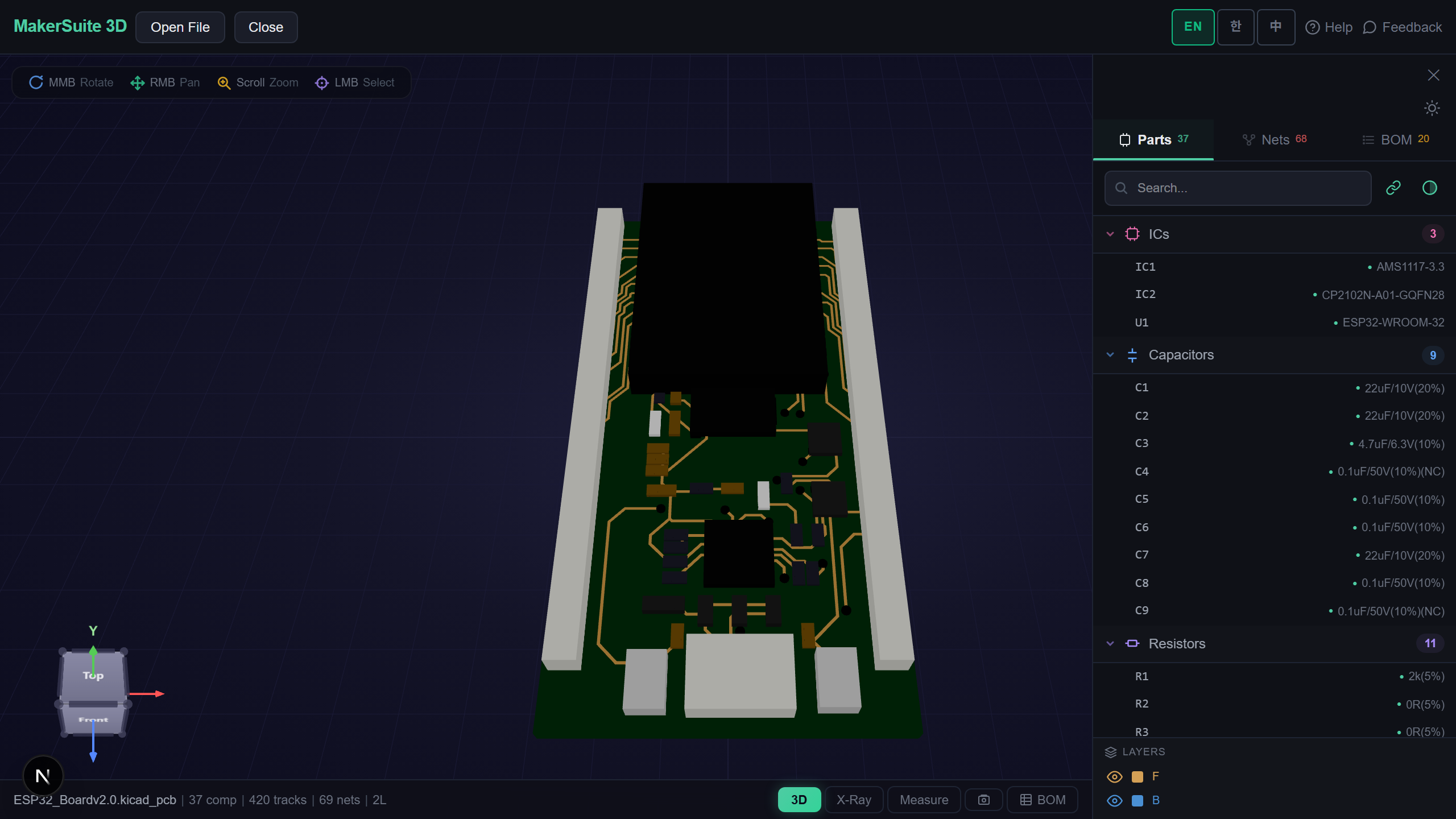
MakerSuite 3D runs the whole check client-side. Drop a KiCad, Gerber, Eagle, EasyEDA, Altium, PADS, P-CAD, Protel 99, Allegro file into the viewer, click DFM in the toolbar, and pick your manufacturer. Nine checks run against that fab's published limits and each one reports the worst measured value, how many features violate it, and the fix. Clicking "Show in 3D" pins every offending feature onto the board so you know where to look when you go back to your EDA tool. Nothing is uploaded — parsing and calculation happen in the tab, which matters if the design is under NDA.
See every limit this checks, side by side →
Read "not evaluated" carefully
A check that reports "not evaluated" is telling you something useful: the file does not contain the data. A Gerber zip exported without the Excellon drill file has no holes to measure, so hole size and annular ring cannot be judged — and reporting those as passing would be worse than useless. The same applies to edge clearance when the outline layer is missing. If you see "not evaluated" on something you care about, the fix is to re-export with that layer included, which is also exactly what the fab would have asked you for.
A one-minute pre-order routine
Before every order: open the exported files in a viewer that renders them independently of your EDA tool — this alone catches missing layers and broken outlines. Run the DFM check against the fab you are actually using, not a generic profile. Fix anything marked as a failure. Note the warnings and decide consciously whether to spin them now or later. Then upload to the fab's own preview, which applies their internal rules on top. Three passes, under a minute each, and the two-day email stops happening.
Frequently Asked Questions
Does passing DRC mean my board is manufacturable?
No. DRC compares the board against the design rules configured in your own project, which by default are whatever shipped with the software template. They encode nothing about the factory you eventually chose. A 6 mil clearance rule passes DRC forever, whether the fab needs 5 mil or 3.5 mil on the layer count you ordered. DRC is still necessary because it catches shorts and unconnected nets that no manufacturability check looks at, but it answers a question about your intent rather than the factory's capability.
What are the most common reasons a fab rejects a board?
Trace width and spacing below the etch limit come first — traces neck or short and no process tuning saves them. Then drill diameter under the mechanical floor, which pushes you to laser microvias at a different price tier. Annular ring is the one people forget: drill placement has tolerance, so too little copper around a via means the bit breaks out through the pad edge and the connection dies. After that, copper too close to the board outline, since routing and V-scoring have tolerance too. Board size and layer count are cheaper mistakes but still block an order — odd layer counts do not exist because stackups are built from bonded pairs.
What is a safe minimum annular ring?
0.13 mm is the standard-process floor at both JLCPCB and PCBWay, computed as (pad diameter − drill) / 2. A 0.6 mm pad over a 0.3 mm drill gives 0.15 mm and is comfortably inside spec; a 0.5 mm pad over a 0.3 mm drill gives 0.10 mm and will be flagged. If you are tight on space, enlarging the pad is almost always easier than shrinking the drill, because the drill has its own separate minimum.
Are silkscreen warnings worth fixing before ordering?
Usually not. Lines thinner than the printer resolves and text below roughly 1 mm come out smudged or missing, which makes reference designators useless during hand assembly and rework — but the board is still fabricated and still works electrically. Treat them as a to-do for the next revision. Copper and drill violations are the opposite: hard stops where the fab either rejects the file or silently substitutes a parameter you never asked for.
How do I check a board without installing anything?
Open the board file in MakerSuite 3D's viewer and click DFM in the toolbar, then pick your manufacturer. Nine checks run against that fab's published limits and each reports the worst measured value, the number of violating features, and the fix. "Show in 3D" pins every offending feature onto the board so you know where to look back in your EDA tool. KiCad, Gerber, Eagle, EasyEDA, Altium, PADS, P-CAD and Protel 99 files all work, and nothing is uploaded — parsing and calculation happen in the browser tab.
Why would a check report "not evaluated"?
Because the file does not carry the data for it. A Gerber zip exported without the Excellon drill file has no holes to measure, so hole size and annular ring cannot be judged, and reporting them as passing would be worse than saying nothing. The same applies to edge clearance when the outline layer is missing. If something you care about shows as not evaluated, re-export with that layer included — which is exactly what the fab would have asked you for anyway.
Related Articles
Stop guessing whether it will pass.
Run a DFM check