발주 전 PCB 제조 가능성 확인하는 법
이틀 뒤에 오는 메일
실패 양상은 늘 똑같습니다. 보드를 마무리하고, DRC를 돌리고, 거버를 내보내고, 업로드하고, 결제합니다. 이틀 뒤 엔지니어에게 메일이 옵니다. 2번 레이어에 최소 선폭 위반이 있다거나, 비아 드릴이 한계보다 작다거나, 구리가 보드 외곽에 너무 가깝다고요. 이제 보드를 다시 돌려야 하고 납기는 처음부터 시작입니다. 그 메일의 내용 중 예측 불가능했던 것은 하나도 없습니다 — 그 한계값은 전부 제조사 웹사이트에 공개돼 있고, 전부 이미 내보낸 파일에서 측정 가능합니다.
DRC 통과가 충분하지 않은 이유
DRC는 프로젝트에 설정된 설계 규칙을 기준으로 보드를 검사합니다. 기본 템플릿에서 시작했다면 그 규칙에는 결국 고르게 된 공장에 대한 정보가 전혀 담겨 있지 않습니다. 클리어런스 6mil 규칙은 제조사가 5mil을 요구하든 3.5mil을 요구하든 영원히 DRC를 통과합니다. 더 나쁜 건, 대부분의 입문자는 설계 규칙 대화상자를 아예 열어보지 않는다는 점입니다. 즉 DRC는 소프트웨어에 딸려 온 숫자를 기준으로 보드를 검증하고 있는 셈입니다. DRC는 필요합니다 — 어떤 제조 가능성 검사도 보지 않는 단락과 미연결 넷을 잡아내니까요. 다만 그것은 공장의 능력이 아니라 내 의도에 관한 질문에 답합니다.
실제로 보드를 반려시키는 수치들
실무에서는 소수의 한계값이 반려의 대부분을 차지합니다. 먼저 최소 선폭과 선간 간격입니다. 에칭 한계 아래로 가면 배선이 잘록해지거나 단락되고, 공정을 아무리 조정해도 살릴 수 없습니다. 다음은 최소 드릴 지름입니다 — 기계 드릴에는 하한이 있고, 그 아래로 가면 가격대가 다른 레이저 마이크로비아로 넘어갑니다. 사람들이 잊는 것이 애뉼러 링입니다. 드릴 위치에는 공차가 있어서, 홀 주위에 남은 구리가 너무 적으면 드릴이 패드 가장자리를 뚫고 나가 연결이 죽습니다. 그다음이 구리-엣지 클리어런스입니다. 라우팅과 V-컷에도 공차가 있어 외곽선 근처의 구리는 깎이거나 박리됩니다. 보드 크기와 레이어 수는 더 값싼 실수지만 여전히 발주를 막습니다 — 적층은 본딩된 쌍으로 만들어지므로 홀수 레이어는 존재하지 않습니다.
미관 문제와 차단 문제 구분하기
모든 경고가 발주를 막아야 하는 건 아닙니다. 실크스크린 문제 — 인쇄 해상도보다 얇은 선, 읽기에 너무 작은 글자 — 는 부품 번호를 뭉개거나 사라지게 만듭니다. 수작업 조립과 리워크에는 실제로 불편하지만, 보드는 그대로 제작되고 동작합니다. 다음 리비전의 할 일로 두세요. 구리와 드릴 위반은 다릅니다. 이건 확실한 정지선이고, 제조사는 파일을 반려하거나 요청하지도 않은 값으로 조용히 대체합니다.
브라우저에서 내 보드를 제조사 한계와 대조해보세요 — 업로드도, 가입도 없습니다.
MakerSuite 3D 무료로 써보기브라우저에서 검증하기
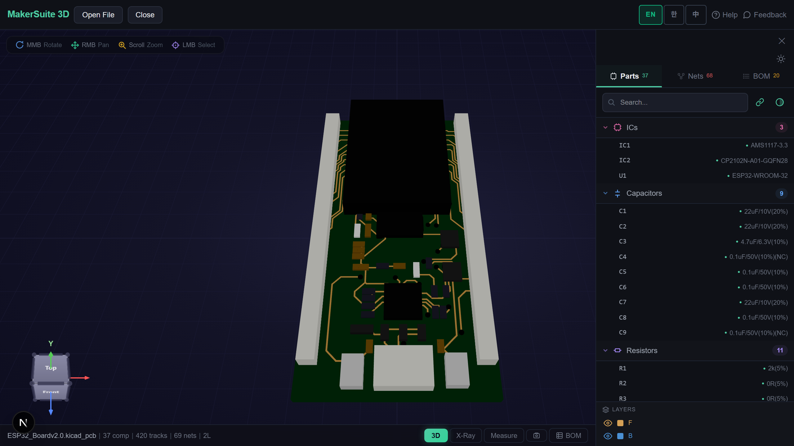
MakerSuite 3D는 이 검사 전체를 클라이언트에서 돌립니다. KiCad, Gerber, Eagle, EasyEDA, Altium, PADS, P-CAD, Protel 99, Allegro 파일을 뷰어에 놓고, 툴바의 DFM을 클릭하고, 제조사를 고르세요. 그 제조사의 공개 한계값을 기준으로 9가지 검사가 돌고, 각 항목이 실측 최악값·위반 개수·해결 방법을 알려줍니다. "3D에 표시"를 누르면 문제가 되는 피처가 전부 보드 위에 찍혀서, EDA 툴로 돌아갔을 때 어디를 봐야 할지 알 수 있습니다. 업로드되는 것은 없습니다 — 파싱과 계산이 탭 안에서 일어나며, 설계에 NDA가 걸려 있다면 이게 중요합니다.
"미평가"를 주의 깊게 읽으세요
"미평가"로 나오는 항목은 유용한 정보를 주고 있습니다. 파일에 그 데이터가 없다는 뜻입니다. Excellon 드릴 파일 없이 내보낸 Gerber 압축본에는 잴 홀이 없으므로 홀 크기와 애뉼러 링을 판정할 수 없고, 이걸 통과로 보고하는 건 쓸모없는 정도가 아니라 해롭습니다. 외곽선 레이어가 없을 때의 엣지 클리어런스도 마찬가지입니다. 신경 쓰는 항목이 "미평가"로 나온다면, 해결책은 그 레이어를 포함해 다시 내보내는 것이고 — 그건 제조사가 어차피 요구했을 바로 그것입니다.
1분짜리 발주 전 루틴
매 발주 전에: 내보낸 파일을 EDA 툴과 독립적으로 렌더링하는 뷰어에서 열어보세요. 이것만으로도 누락된 레이어와 깨진 외곽선을 잡습니다. 일반 프로파일이 아니라 실제로 쓰는 제조사를 기준으로 DFM 검사를 돌리세요. 실패로 표시된 것은 고치세요. 경고는 기록해두고 지금 반영할지 나중에 할지 의식적으로 정하세요. 그다음 제조사 자체 프리뷰에 업로드하면 그들의 내부 규칙이 한 번 더 적용됩니다. 각 1분 이하의 세 단계면, 이틀 뒤의 그 메일은 더 이상 오지 않습니다.
자주 묻는 질문
Does passing DRC mean my board is manufacturable?
No. DRC compares the board against the design rules configured in your own project, which by default are whatever shipped with the software template. They encode nothing about the factory you eventually chose. A 6 mil clearance rule passes DRC forever, whether the fab needs 5 mil or 3.5 mil on the layer count you ordered. DRC is still necessary because it catches shorts and unconnected nets that no manufacturability check looks at, but it answers a question about your intent rather than the factory's capability.
What are the most common reasons a fab rejects a board?
Trace width and spacing below the etch limit come first — traces neck or short and no process tuning saves them. Then drill diameter under the mechanical floor, which pushes you to laser microvias at a different price tier. Annular ring is the one people forget: drill placement has tolerance, so too little copper around a via means the bit breaks out through the pad edge and the connection dies. After that, copper too close to the board outline, since routing and V-scoring have tolerance too. Board size and layer count are cheaper mistakes but still block an order — odd layer counts do not exist because stackups are built from bonded pairs.
What is a safe minimum annular ring?
0.13 mm is the standard-process floor at both JLCPCB and PCBWay, computed as (pad diameter − drill) / 2. A 0.6 mm pad over a 0.3 mm drill gives 0.15 mm and is comfortably inside spec; a 0.5 mm pad over a 0.3 mm drill gives 0.10 mm and will be flagged. If you are tight on space, enlarging the pad is almost always easier than shrinking the drill, because the drill has its own separate minimum.
Are silkscreen warnings worth fixing before ordering?
Usually not. Lines thinner than the printer resolves and text below roughly 1 mm come out smudged or missing, which makes reference designators useless during hand assembly and rework — but the board is still fabricated and still works electrically. Treat them as a to-do for the next revision. Copper and drill violations are the opposite: hard stops where the fab either rejects the file or silently substitutes a parameter you never asked for.
How do I check a board without installing anything?
Open the board file in MakerSuite 3D's viewer and click DFM in the toolbar, then pick your manufacturer. Nine checks run against that fab's published limits and each reports the worst measured value, the number of violating features, and the fix. "Show in 3D" pins every offending feature onto the board so you know where to look back in your EDA tool. KiCad, Gerber, Eagle, EasyEDA, Altium, PADS, P-CAD and Protel 99 files all work, and nothing is uploaded — parsing and calculation happen in the browser tab.
Why would a check report "not evaluated"?
Because the file does not carry the data for it. A Gerber zip exported without the Excellon drill file has no holes to measure, so hole size and annular ring cannot be judged, and reporting them as passing would be worse than saying nothing. The same applies to edge clearance when the outline layer is missing. If something you care about shows as not evaluated, re-export with that layer included — which is exactly what the fab would have asked you for anyway.
관련 글
통과할지 짐작하지 말고 확인하세요.
DFM 검사 실행